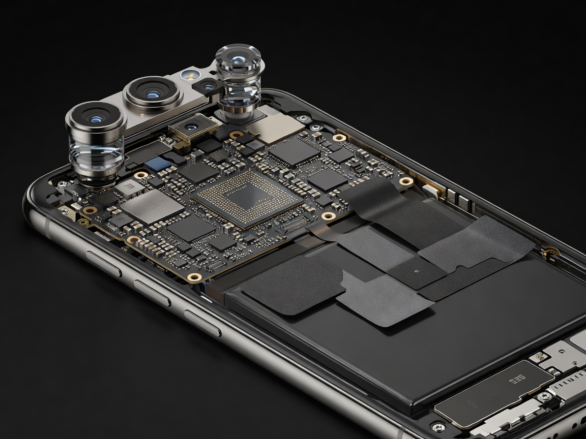
Semiconductor Lithography and Thermal Realities
Modern System-on-Chip (SoC) architectures integrate billions of transistors on nanometer-scale fabrication nodes. As transistors decrease in size, electrical resistance produces intense localized heat. Because smartphones lack mechanical fans, this thermal energy must transfer passively through graphite sheets and vapor chambers to the exterior frame.
When a phone undergoes heavy computational load—such as running localized language models or recording high-framerate 4K video—it eventually hits thermal limits. The operating system responds with thermal throttling, reducing processor clock frequencies to protect the lithium battery chemistry from degradation.
Display Technology: LTPO and Power Management
The screen remains the single largest battery drain in typical daily smartphone usage. Low-Temperature Polycrystalline Oxide (LTPO) backplane technology transforms this dynamic by dynamically shifting the refresh rate from 120Hz down to 1Hz based on displayed content.
Why Adaptive Refresh Matters
When reading a static editorial article or reviewing an eBook, the screen draws energy once per second instead of 120 times. This preserves power for background computational tasks and ensures smoother transitions when scrolling resumes.
Camera Hardware vs. Computational Photography
Smartphone camera lenses are physically constrained by device thickness. Flagship hardware overcomes this optical barrier through folded periscope optics and larger 1-inch-type image sensors.
However, the raw photon capture is only the starting point. When you press the shutter, the Image Signal Processor (ISP) captures a rapid burst of multiple underexposed and overexposed frames, fusing them in memory within fractions of a second to eliminate motion blur and expand dynamic range.
| Hardware Component | Core Function | Modern Technological Milestone | Direct User Benefit |
|---|---|---|---|
| Unified Memory (LPDDR5X) | Shared high-bandwidth data pool | 12GB to 16GB standards | Zero-copy access for CPU, GPU, and NPU |
| Vapor Chamber Cooling | Phase-change heat dissipation | Expanded titanium-bonded plates | Prevents early thermal throttling |
| UFS 4.0 Storage | High-speed flash read/write | Multi-lane bandwidth throughput | Instantaneous app launch and video caching |
Security Enclaves and Biometrics
Security on modern smartphones is rooted in isolated silicon enclaves. These dedicated hardware microprocessors run an isolated microkernel separate from the primary operating system.
Your biometric fingerprints, facial depth maps, and encryption keys never reside in general system memory. Even if an attacker gains root access to the operating system, the secure enclave refuses to surrender cryptographic private keys, rendering extracted device dumps useless.
What to Know:
- High megapixel counts do not equal superior image fidelity; physical sensor area and aperture size remain decisive.
- Peak brightness ratings measured in thousands of nits apply only to tiny window percentages during HDR playback, not continuous full-screen daylight use.
- RAM capacity directly determines how many heavy applications stay alive in background memory without forcing reload cycles.